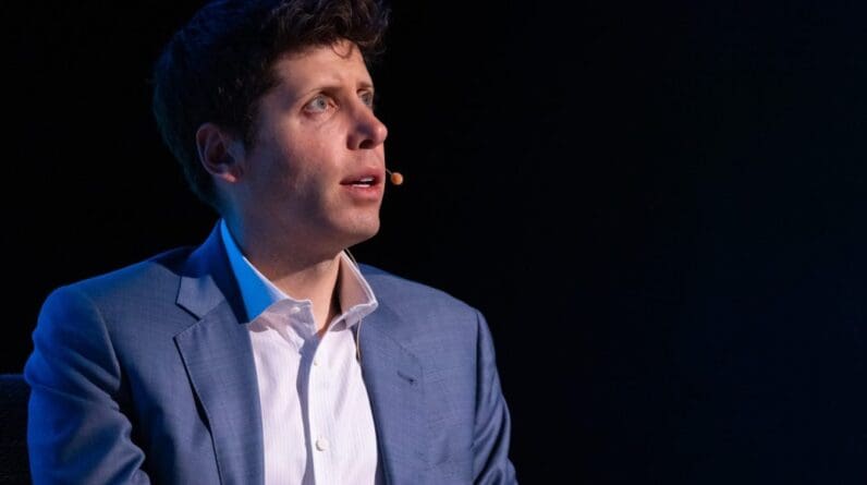
OpenAI Chief Executive Officer Sam Altman is visiting leaders of South Korea’s semiconductor industry this week, as the artificial-intelligence pioneer weighs an ambitious move into chip production.
Altman, who arrived in Seoul Thursday evening, is touring Samsung Electronics Co.’s chip fabrication plants in Pyeongtaek on Friday, according to a person familiar with the matter. He’ll meet the top executive of Samsung’s semiconductor business, as well as divisional heads of the foundry, memory and system LSI units, said the person, who asked not to be named as the matter is private. He is also scheduled to meet the CEO of rival SK Hynix Inc. and SK Group Chairman Chey Tae-won to discuss ways to collaborate, the person said.
Since OpenAI released ChatGPT more than a year ago, interest in AI applications has skyrocketed, spurring massive demand for the computing power and processors needed to build and run those AI programs. Altman has repeatedly said there already aren’t enough chips for his company’s needs.
It’s not clear what the goals of Altman’s Korea trip are. He has been working to raise billions of dollars to set up a network of factories to manufacture semiconductors, Bloomberg News reported this month. Samsung has been expanding its foundry business, which manufactures chips to the designs of its customers.
Representatives for Samsung and SK Hynix declined to comment. OpenAI representatives didn’t immediately respond to requests for comment.
South Korea is a leader in high-end chip production, dominating the market with Taiwan. Taiwan Semiconductor Manufacturing Co. is the leading foundry in the world, crafting chips for the likes of Apple Inc. and Nvidia Corp.
The Korean government this month outlined a blueprint involving investment of 622 trillion won ($466 billion) from the private sector in the years leading up to 2047. They will spend the money to build 13 new chip plants and three research facilities, on top of an existing 21 fabs. Spanning Pyeongtaek to Yongin, the area is expected to be the largest in the world, capable of producing 7.7 million wafers monthly by 2030.
The world’s two biggest memory chipmakers are trying to build their most sophisticated chip plants at home. Samsung is betting big on the foundry expansion as part of a 500 trillion won investment by 2047. SK Hynix aims to invest 122 trillion won in memory in Yongin over the same period.


